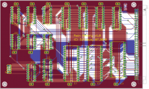
I ran out of kynar wire and was forced to take a break from wrapping so I decided to take this opportunity and design a custom PCB for my memory module. Since this was my first attempt to lay out a board, it took me over a week – much longer than I had expected (yes, I still have time for the project only on weekday evenings). My kynar roll arrived long time ago, but only now I am ready to send the board design to the fab house and return to wrapping (which I already hate).
The reason it took me so long is that I was constantly unhappy with the way the boards ultimately looked and the number of vias it required after autorouting (initially my attempts called for 200+ vias). My approach was to lay out the components manually, with some assistance of the schematic diagrams (to place related components close to each others). Somehow, I am still having trouble using airwires for this purpose – they are just too many for me to be able to find a correct layout using only them (especially when multiple airwires run in parallel). I had the impression that all my parts had airwires leading to almost all remaining components on the board. This irritated me, so I was attempting layout after layout after layout. Also, I was routing power lines manually. Eagle autorouter would route them randomly with respect to power filter caps, which was not what I wanted. However, my manual routing occupied to much board space and set multiple obstacles the autorouter had to jump over using vias. Ultimately, I routed power vertically on the to side of the board, ground horizontally on the bottom side of the board and ran the autorouter with the setting to optimize for the same alignment. The via count (my board quality indicator) went down from 200+ to something around 40. Finally, I was satisfied. So, here is my first ever PCB (click to enlarge).
As previously announced, I used Eagle non-profit version. The board is 100x160mm (standard eurocard size) and is intended for installation in standard 19-inch rack (3U). Ultimately, the entire computer will sit in such rack, and boards will be connected using a 64-wire ribbon cable. You can see a ribbon connector sticking out the right side of the board.
Preparing a board design required some changes to the schematic. These are rather editorial than functional. Schematics required adding a ribbon connector and board headers, nothing particularly interesting. I have also split the memory schematics into base part (corresponding the the 1MB base memory board) and 3MB memory expansion. Eagle files are available for download here.
The tricky part on the board I am especially proud of is that it is expandable. If you recall my memory design, it allows for maximum 4MB of memory (22-bit physical address bus). But the board contains only one 128kB ROM chip and two 512kB SRAM chips. The idea here is to make another board, which will contain extended memory, and whose chip sockets will be in line with SRAM sockets on the main memory board (the one above). One of the sockets will have longer leads (like those for wire wrapping). This way, I can remove one of the SRAM chips from the main board, and stack the expansion board on top of it, connecting the wire wrap socket’s leads from the expansion board to the freed socket on the main board. This will transfer the address bus and data bus lines to the expansion board, /ENMEM and /LDMEM signals, and the chip select signal of the SRAM chip relocated from the main board to the expansion board. The remaining chip select signals (plus power and ground) will be transferred via JP1 header connector, which will have its long pins counterpart on the expansion board, in the exact same location in reference to board edges. To secure everything and make sure it does not fall apart easily, both boards will be additionally held together using 15mm posts and M3 screws (hence the holes in board corners).
For practical reasons, in order not to leave ROM on the lower board of the stack, I will probably do similar repositioning of the ROM chip (i.e. remove it from the lower board and provide a socket for it on the expansion board in the exact same location but with longer pins). This way ROM will be easily accessible for reprogramming. If you look at the board you will notice that I have left enough room around the ROM chip in order to use a ZIF socket to easily plug and unplug it.
As far as board house is concerned, I will use BatchPCB (www.batchpcb.com) since they are probably the cheapest around. My board is $74 to manufacture and ship, and prices for this size board at European board houses were all 70-100 euros. The only drawback of BatchPCB is that you usually wait long to get your board as these guys wait until they fill the entire panel with orders before they submit their bulk order to their vendor in China. I still have a lot of wire wrapping in front of me so that’s not a big issue, though. I can wait.
