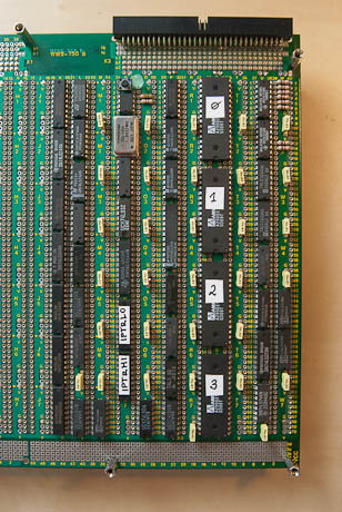
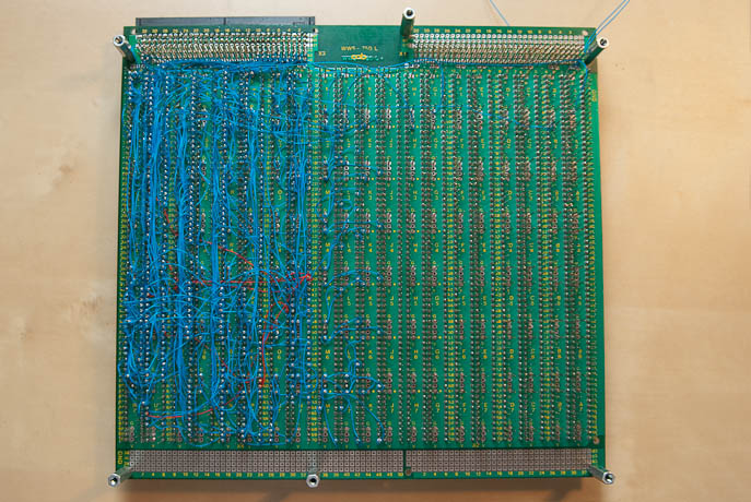
Not much to celebrate, progress is still slow. I am working on the project only in short evening sessions, and spending time on other stuff on weekends. The current status is that I have completed the control module wiring, and placed MSW and bus interfaces components on the board. Next, I will continue wiring these modules and then I work on the register set (not yet on the board). This should complete the main board. Below are the most recent photos of it, taken from both sides.


The completed control module is the tangle of blue wires on the left of the board. Few wires are red – these are the clock signals which I wanted to have visible to make sure they are not running in parallel to each other (or other wires) which could cause unwanted crosstalk. I connected the CPU in its current state it to the logical analyzer and made a few tests. For now, everything seems to be working fine – the reset sequence was OK, the microcode step counters and the priority encoders behaved as expected. The machine is able to run an endless loop of NOPs when it is on (NOP opcode is $00 and this is exactly the value on the data bus that does not exist). So, in some way, my CPU already boots.
 As said in one of the previous posts, there will be another wire wrapped board to hold the ALU. Unfortunately, there is not enough room on the main board to fit the ALU there, hence another board. Looking at the current board layout I figure I could have packed the ICs more densely, which (with a bit of luck) would allow me to cram everything in, including the ALU. However, this would be at the expense of power filter caps (my wire wrap board does not have dedicated rows for capacitors, unlike some boards I have seen), which could eventually degrade the overall system stability. I hope that ALU will be the last wire wrapped board I ever have to make, though.
Memory is a different story. Since memory is isolated and independent from the CPU (well, almost) I will make a custom PCB to hold the memory module. Preliminary component count and layout attempt indicated that I will need two stacked euro-size (160 x 100 mm) boards for this. Ultimately, the entire CPU will also consist of several PCBs (I am assuming wire-wrap to be a prototype stage only) and I will reuse the memory board with the “production” board-based CPU later. I just need to plan the backplane bus connector carefully so that I don’t need to change the signal assignments in the future. I think the memory module is simple enough to get started with the PCBs and will be a good exercise. I have never made a PCB before, but if I manage to do it correctly, the memory module alone will save me a lot of wire-wrapping pain.
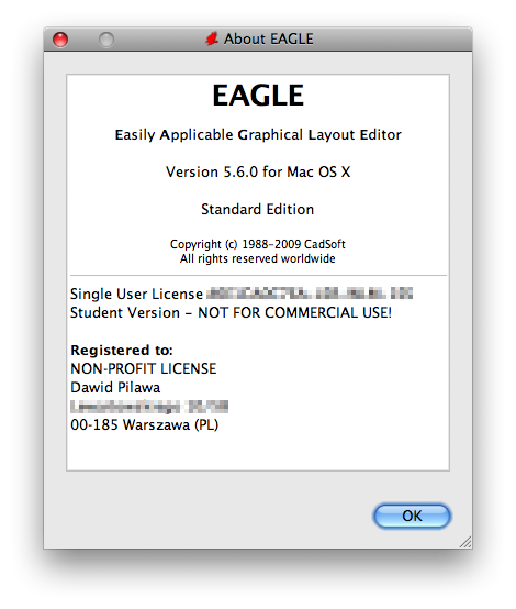
To design the PCBs I have purchased a non-profit EAGLE license for 125 euros from CadSoft in Germany. It is a fully-featured license, with all application capabilities, but intended for educational purposes and for only one user. That’s a good value for money, considering that a regular license providing the same functionality costs several hundred euros.
Regardless of my ambitious plans, considering my current pace it looks like there is still a few weeks of wire wrapping to come. I tried looking for a faster cut-strip-wrap bit for my electric tool on eBay but unfortunately could not find one. And a brand new one from Cooper costs over $700 (!). Looks like I have to do with what I have and use some more patience.