This is what an assembled stack of seven CPU boards looks like. I was able to complete the soldering work recently, and now have a complete CPU and a bunch of peripherals on printed circuit boards. Farewell, old wire-wrapped CPU prototype! The new CPU is way more robust than the delicate wire mesh. It is also more compact and will not occupy most of my desk space whenever I want to tinker with it.
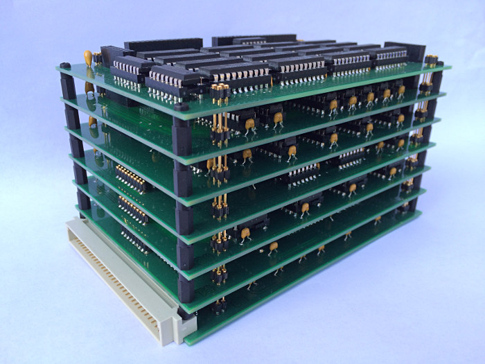
Each of the boards took around 3 hours of assembly work. I started with soldering all passive components, then I soldered precision sockets, and finally stackable headers. I used these (very expensive) breakable machined headers for my power and ground rails (I was not able to find 2×2 stackable headers which I needed) and standard (dirt cheap) stackable Arduino headers like these for remaining board-to-board connectors. Since I have multiple 2×8, one 2×16 and one 2×24 pin headers on my boards, I bought a 100 pcs pack of 1×8 stackable headers on eBay in a belief that I would be able to easily place them next to each other for whatever multiple-of-eight header dimension I needed. I am not sure if these headers are always of such inferior quality or I was unlucky picking a wrong supplier, but this part gave me most headaches and was most labor-intensive. Because of their manufacturing process, these connectors have some excess plastic on their shorter edges so I had to manually sand it off for each of around 90 pieces I used. Having prepared and soldered all headers, a final step was to clean the board with isopropanol (IPA), which was not entirely hassle-free, neither. It was difficult to get in between long header pins with a brush and remove all flux residue.
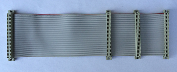
I also crimped a new backplane ribbon because the old one used a combination of DIN 41612 C-Type and standard IDC connectors which were my initial choice for the wire-wrapped CPU. The new one I made 30 cm long (1 ft) which should give me enough room for expansion without making the signal lines excessively long. It is now entirely built of DIN 41612s.
I have been connecting power to the stack upon completion of each board to check for any obvious problems and observed a few critical signals on a scope. They looked relatively clean so I am hoping not to run into significant noise problems or alike. Nevertheless, there are so many things that could have gone wrong if you consider completely new and untested board layouts, my spot checked hand assembly, or possible broken TTL chips (I had to use a few salvaged ones whenever new ones were not available anymore). I will hook up the entire thing today and see if I was lucky. If not, I am up to some interesting debugging work.